原文
GPT Image 2 · en
Scene:
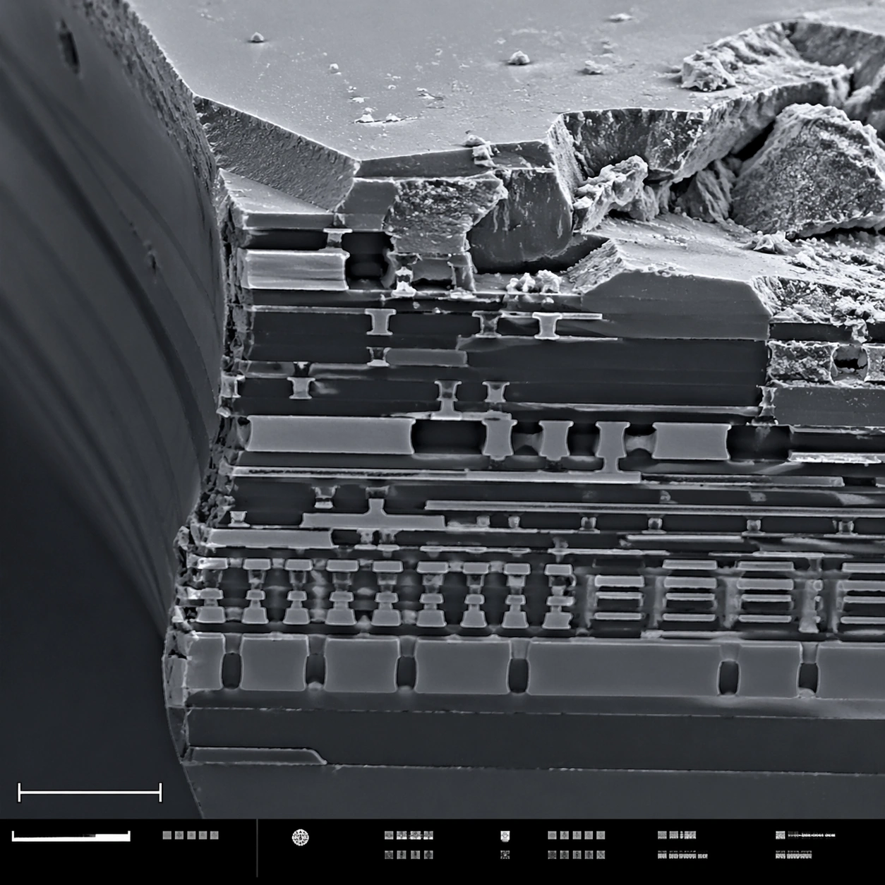
A square scanning electron microscope plate of a fractured microchip cross-section, rendered in sharp monochrome with a slight graphite-blue tint in the shadows. The specimen occupies the main field like a miniature canyon of engineered layers. A lower-left scale bar shape and a bottom instrument-information strip with small unreadable marks make the layout feel like an SEM capture screen.

Subject:
A broken silicon microchip edge at high magnification. Visible features include stacked metal interconnect layers, etched trenches, dielectric strata, jagged fracture planes, tiny vias, rectangular circuit terraces, and granular debris on the cleaved surface. Some layers are smooth and engineered; others are rough and torn, showing contrast between manufactured precision and brittle breakage.

Important details:
Keep the image scientifically plausible and technical. Do not show a normal circuit board or macro electronics; this is a microscopic cross-section. Emphasize SEM relief: crisp edges, grainy fracture texture, deep shadowed trenches, and thin layer boundaries. The structured layout should have a clean main field, scale bar geometry, and bottom strip without readable typography. The image should feel suitable for a failure-analysis report while remaining visually striking.

Use case:
SEM Microscopy single study 8/8, testing technical material SEM realism and structured plate composition.

Constraints:
No readable text, no watermark, no logos, preserve exact 1:1 aspect ratio, no brand marks, no normal macro circuit board, no glowing neon traces, no floating labels, no colorful cyberpunk style, no schematic overlay, no perfect 3D render look.
使い方
- パラメータを含む元のプロンプト全体をコピーします。
- 被写体、文字、構図を自分の要件に置き換えます。
- 対応する外部ツールで使用し、利用条件と結果を確認します。
開始前の確認
- 参考画像の要否を確認してください。互換モデルの表示は、そのモデルでの生成実績を意味しません。
- 名前、数値、画像内の文字を確認します。モデルの版で結果は変わります。