原始文档
GPT Image 2 · en
Scene:
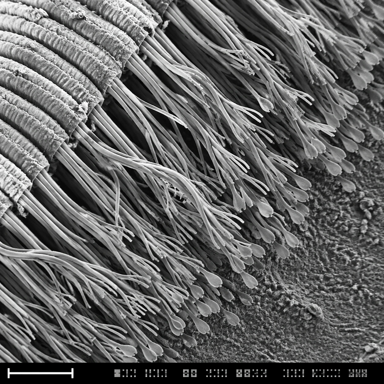
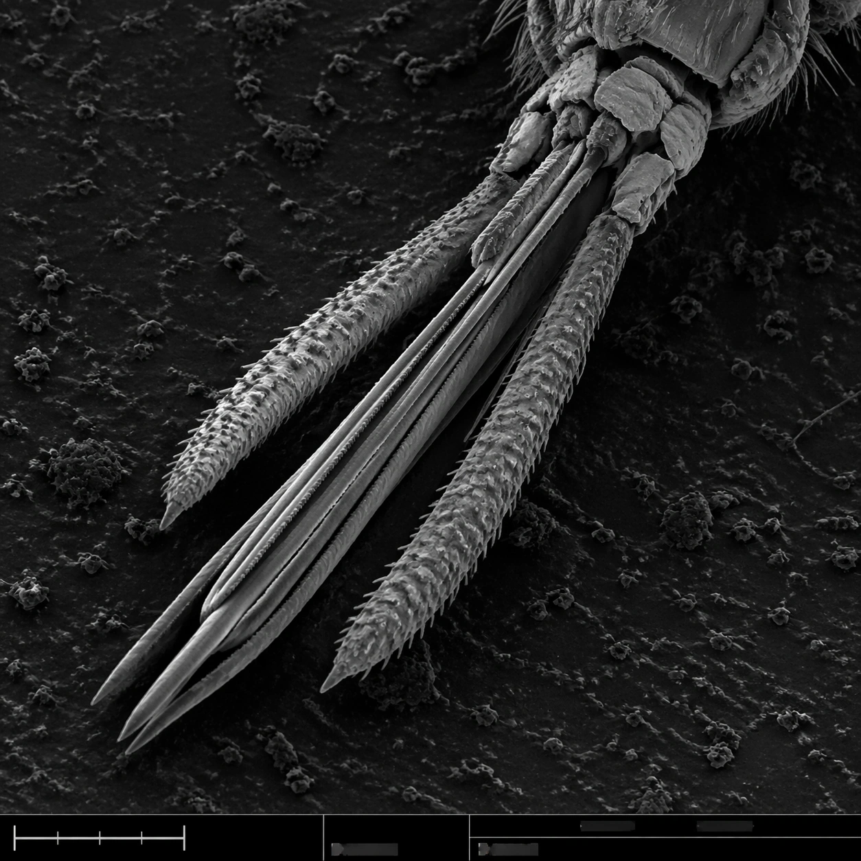
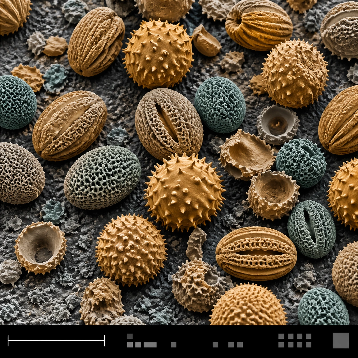
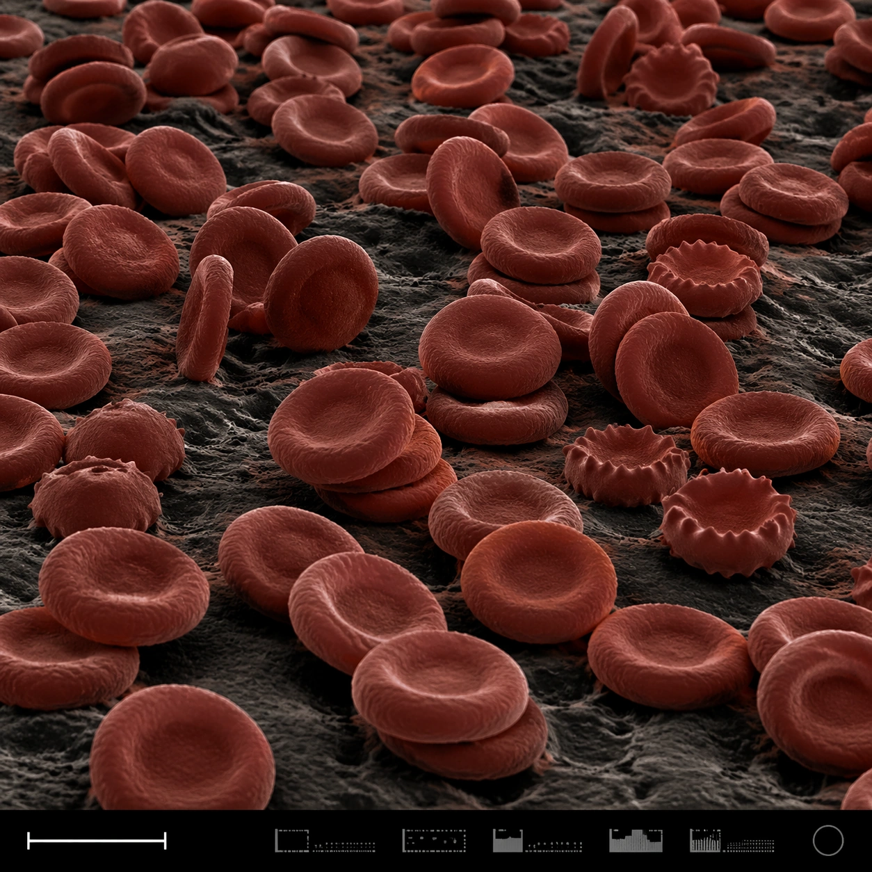
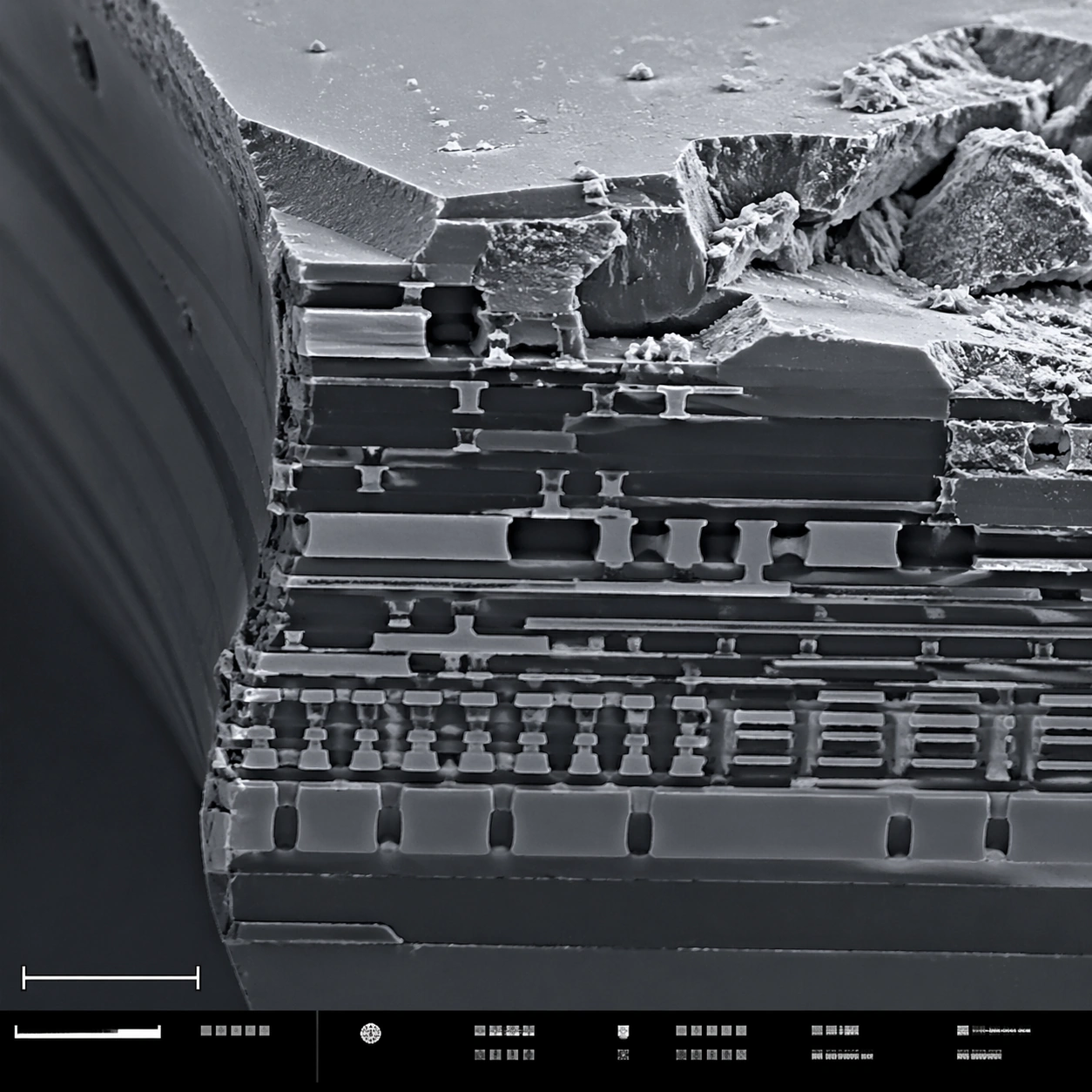
A square scanning electron microscope plate of a fractured microchip cross-section, rendered in sharp monochrome with a slight graphite-blue tint in the shadows. The specimen occupies the main field like a miniature canyon of engineered layers. A lower-left scale bar shape and a bottom instrument-information strip with small unreadable marks make the layout feel like an SEM capture screen.

Subject:
A broken silicon microchip edge at high magnification. Visible features include stacked metal interconnect layers, etched trenches, dielectric strata, jagged fracture planes, tiny vias, rectangular circuit terraces, and granular debris on the cleaved surface. Some layers are smooth and engineered; others are rough and torn, showing contrast between manufactured precision and brittle breakage.

Important details:
Keep the image scientifically plausible and technical. Do not show a normal circuit board or macro electronics; this is a microscopic cross-section. Emphasize SEM relief: crisp edges, grainy fracture texture, deep shadowed trenches, and thin layer boundaries. The structured layout should have a clean main field, scale bar geometry, and bottom strip without readable typography. The image should feel suitable for a failure-analysis report while remaining visually striking.

Use case:
SEM Microscopy single study 8/8, testing technical material SEM realism and structured plate composition.

Constraints:
No readable text, no watermark, no logos, preserve exact 1:1 aspect ratio, no brand marks, no normal macro circuit board, no glowing neon traces, no floating labels, no colorful cyberpunk style, no schematic overlay, no perfect 3D render look.
使用方法
- 复制完整原始提示词,并保留其中的参数。
- 按需求替换主体、文字和构图要求。
- 在兼容的外部工具中使用,核对当前使用条件并检查结果。
开始前需了解
- 先确认是否需要参考图。标注兼容模型,不代表该示例由这个模型生成。
- 核对名称、数字与画面文字;不同模型版本的结果可能不同。