원본 문서
GPT Image 2 · en
Scene:
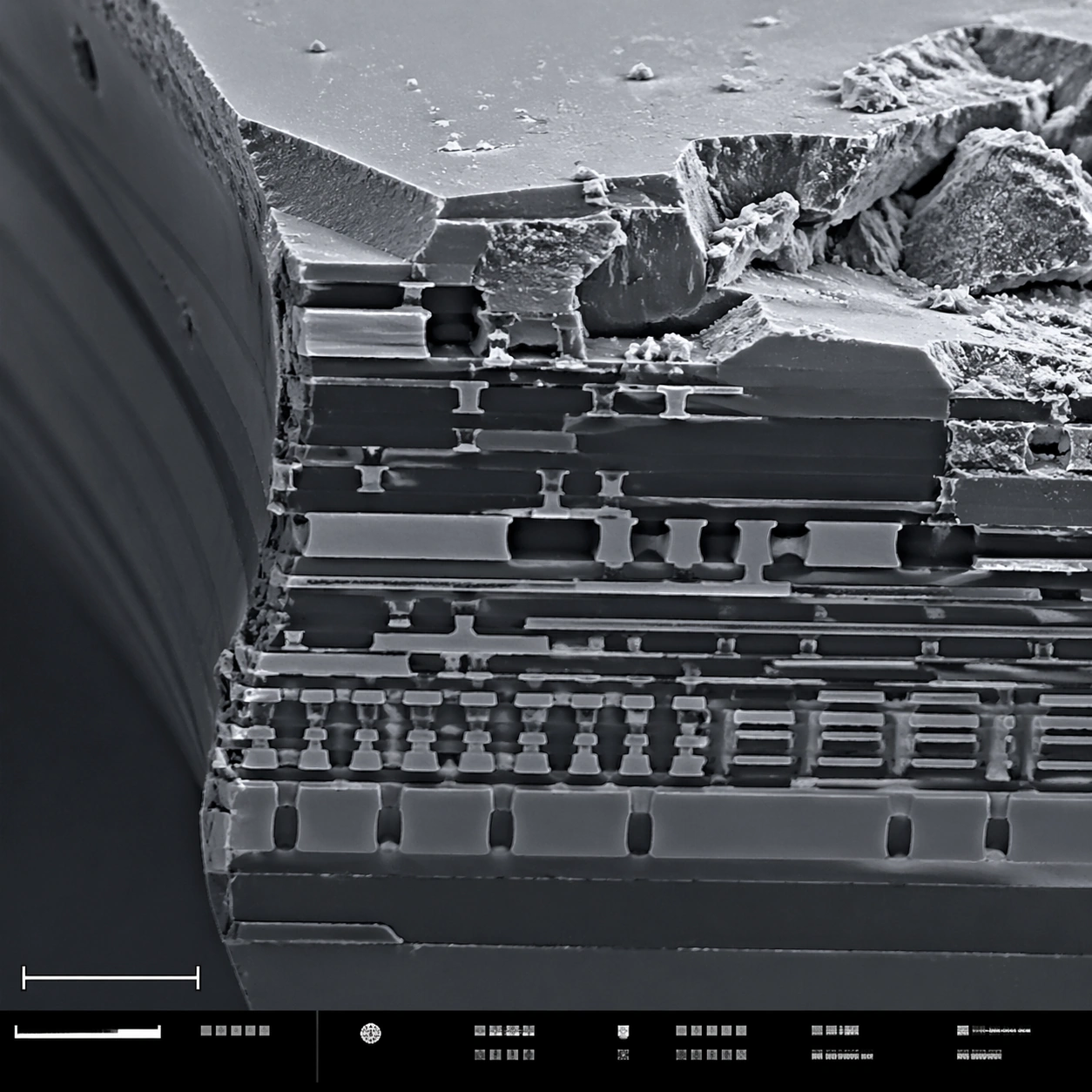
A square scanning electron microscope plate of a fractured microchip cross-section, rendered in sharp monochrome with a slight graphite-blue tint in the shadows. The specimen occupies the main field like a miniature canyon of engineered layers. A lower-left scale bar shape and a bottom instrument-information strip with small unreadable marks make the layout feel like an SEM capture screen.

Subject:
A broken silicon microchip edge at high magnification. Visible features include stacked metal interconnect layers, etched trenches, dielectric strata, jagged fracture planes, tiny vias, rectangular circuit terraces, and granular debris on the cleaved surface. Some layers are smooth and engineered; others are rough and torn, showing contrast between manufactured precision and brittle breakage.

Important details:
Keep the image scientifically plausible and technical. Do not show a normal circuit board or macro electronics; this is a microscopic cross-section. Emphasize SEM relief: crisp edges, grainy fracture texture, deep shadowed trenches, and thin layer boundaries. The structured layout should have a clean main field, scale bar geometry, and bottom strip without readable typography. The image should feel suitable for a failure-analysis report while remaining visually striking.

Use case:
SEM Microscopy single study 8/8, testing technical material SEM realism and structured plate composition.

Constraints:
No readable text, no watermark, no logos, preserve exact 1:1 aspect ratio, no brand marks, no normal macro circuit board, no glowing neon traces, no floating labels, no colorful cyberpunk style, no schematic overlay, no perfect 3D render look.
사용 방법
- 매개변수를 포함한 전체 원본 프롬프트를 복사하세요.
- 주제, 문구, 구도를 자신의 요구에 맞게 바꾸세요.
- 호환되는 외부 도구에서 사용하고 이용 조건과 결과를 확인하세요.
시작 전 확인
- 참조 이미지가 필요한지 확인하세요. 호환 표시는 해당 모델로 이 예시를 생성했다는 뜻이 아닙니다.
- 이름, 수치, 이미지 속 문구를 확인하세요. 모델 버전에 따라 결과가 다를 수 있습니다.