
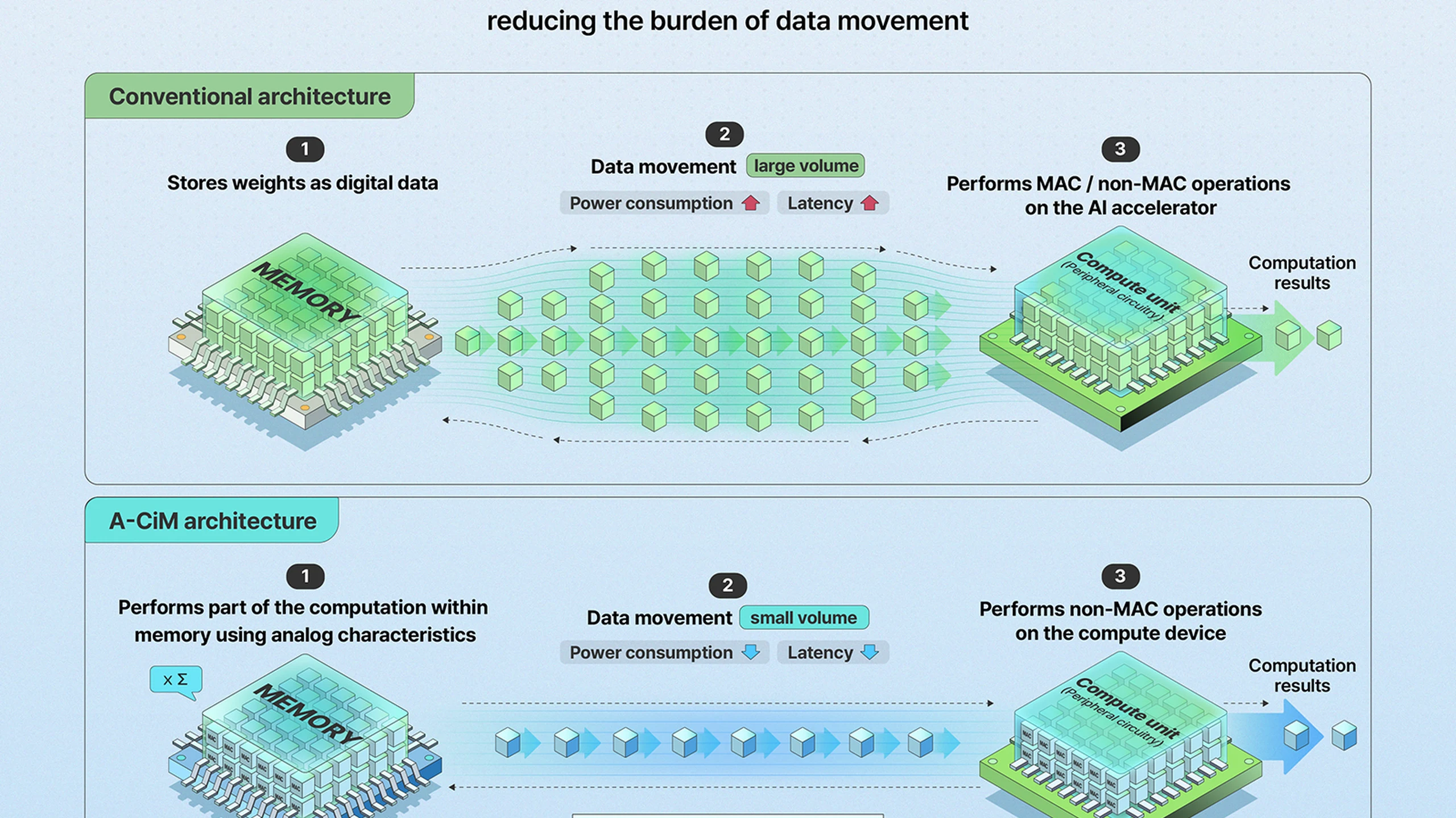
SK hynix is trying to change where AI arithmetic happens, not merely how much data a NAND device can hold. Its latest public explanation of 3D FeNAND describes keeping model weights in vertically stacked memory and performing selected multiply-and-accumulate operations there. The potential saving comes from avoiding repeated transfers to a separate processor.
The October 14, 2026 account explains research presented at IEDM in December 2025. It reports striking gains, but no commercial chip, production date or customer qualification program. The useful development is a coordinated design of memory cells, supporting controls and workload placement—not a claim that an ordinary SSD can replace a GPU.
Two comparisons that must not become one promise
The company's account reports up to 16 times higher throughput and 4,950 times higher energy efficiency than selected conventional two-dimensional arrays under its evaluated workload and constrained chip-area assumptions. Those are architecture comparisons, not universal multipliers for an entire AI server.
A technical summary uses a different reference: the earlier 3D FeNAND design. Against that predecessor, co-optimization delivered 20.4 times more TOPS and 7.17 times more TOPS per watt. TOPS denotes trillions of operations per second; TOPS/W describes energy efficiency. The two baselines cannot be combined or exchanged.
High density helps explain why the energy improvement against a planar array can greatly exceed the throughput improvement. When more weights fit locally, fewer reloads, rewrites and idle periods surround the calculation. But the saving depends on the model and mapping; it does not establish a measured 4,950-fold reduction in a production system's electricity bill.
Three linked changes make the density usable
FeNAND uses ferroelectric polarization that remains after an electric field is removed. That state controls cell current and can encode multiple nonvolatile weight levels. Conventional commercial 3D NAND generally uses charge-trap nitride, storing electrons in an insulating layer. Dense digital storage and precise analog current control are different engineering requirements.
A long vertical string adds resistance. Current flowing through it creates an IR drop—a voltage loss that can compress the separation between analog states. Closely spaced states are harder to distinguish, so packing more cells is not automatically equivalent to obtaining more accurate computation.
At the cell level, SK hynix uses pulse-number modulation: a controlled sequence of programming pulses tunes the stored states under low-current, IR-drop-aware conditions. This is a multilevel programming method, rather than simply a faster transistor. It addresses the usable current range on which analog weights depend.
The second change concerns non-cell overhead. Word lines select and control cells, and repeatedly changing their voltages consumes energy and time. Dual-word-line activation reduces the transition burden. Treating those controls as part of the computation matters because an efficient cell can otherwise be surrounded by expensive switching.
The third change is page organization. In-page pipelining places multiple neural-network layers and duplicates selected operations within a page, reducing forward operations and word-line transitions. Page splitting compares a 16 KB page with a 4 KB arrangement to better match the workload. An oversized page activates unused circuitry; an undersized page may require extra operations.
The paper, listed in the IEDM program, therefore links cell, non-cell and page schemes. Vertical capacity becomes valuable only if programming, switching and mapping allow useful work to exploit it.
The memory wall does not disappear everywhere
The in-memory computing literature identifies data movement as a substantial time and energy cost. Analog arrays exploit physical currents to multiply inputs by stored weights and sum results in parallel. Retaining a large weight set nearby can reduce traffic through storage, DRAM, caches and an accelerator.
Stable-weight inference is a plausible initial fit. Training involves frequent updates, precision requirements and flexible execution that are harder to accommodate. HBM and GPUs are not made redundant: HBM can serve changing activations and general accelerator traffic while a dense FeNAND tier handles suitable fixed-weight operations.
Other approaches face different compromises. SRAM is fast and compatible with logic processes but volatile and relatively area-intensive. RRAM crossbars offer programmable resistance but confront variation, endurance and conversion overhead. Phase-change and magnetic memories also balance density, speed and reliability; digital near-memory logic offers more predictable precision, potentially with smaller efficiency gains.
At IEDM 2025, Macronix described mixed-mode 3D NAND in-storage computing for LLMs, using Qwen 2.5 Math 7B and MATH500 to evaluate errors. That is neighboring research, not a direct benchmark validating SK hynix's results. Likewise, the earlier IEEE FeNAND overview reported at least 256 conductance levels and 87.8% accuracy in its evaluated task; it is not an accuracy claim for a current language model or this new architecture.
Accuracy and peripheral costs decide the practical gain
Analog parallelism trades some digital certainty for physical efficiency. Noise, process variation, circuit effects and conversion error affect results, as discussed in the analog accuracy review. Adding correction may improve precision while consuming the area, time or energy that the architecture aims to save.
FeNAND also has vertical-string resistance, neighboring-cell interactions and switching-threshold variation to manage. Ferroelectric retention, repeated-programming endurance, drift and temperature sensitivity must remain acceptable across large arrays. Increasing the number of weight levels narrows the margin between them, making these effects more consequential.
A deployable accelerator must count analog-to-digital converters, input delivery, accumulation of partial results, scheduling and host communication. Cooling and power delivery add further costs. Without comparable boundaries, an array-level TOPS/W figure and a whole GPU system measurement answer different questions.
Software is equally material. Compilers must map operations to available pages, precision and current levels; calibration must preserve useful accuracy. Changes in attention mechanisms, sparsity or quantization may arrive faster than a new fabrication process. A design needs enough programmability to remain useful when its original workload changes.
What would turn the research into a product case
The next convincing evidence would be a fabricated co-optimized chip reporting accuracy alongside throughput and energy, including converters and peripheral logic. Measurements across temperatures and multiple chips would show whether results survive beyond favorable conditions. Current-model tests should disclose size, precision, weight updates, page placement and reload frequency.
Manufacturing evidence must then address ferroelectric process integration, yield, retention and endurance, supported by developer tools and an accelerator partner or evaluation platform. None of those milestones is supplied by an efficiency multiplier alone. The present result is a research advance toward specialized inference, not a purchasing specification.
For teams tracking the field, preserving papers and benchmark definitions in a searchable technical-document knowledge base can help keep these comparisons straight. The decisive question is whether density still saves energy once accuracy, software and all the surrounding hardware are measured together.